Test grating TGQ1 is intended for:
- simultaneous calibration in X, Y and Z directions;
- lateral calibration of SPM scanners;
- detection of lateral non-linearity, hysteresis, creep and cross-coupling effects.
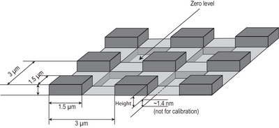
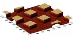
Grating description
|
Structure |
- Si wafer |
|
Pattern types |
3-Dimensional array of small rectangles |
|
Period |
3.0±0,05 µm |
|
Height |
20nm ±1,5 nm* |
|
Rectangles side size: |
1,5±0,35 µm |
|
Chip size |
5x5x0,5 mm |
|
Effective area |
central square 3x3 mm |
* the average meaning based on the measurements of 5 gratings (from the batch of 300 gratings) by SPM calibrated by PTB certified grating TGZ1. Basic step height can vary from the specified one within ±10% (for example step height can be 22±1.5nm)
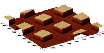
Fig.1 SPM image of TGQ1 grating