


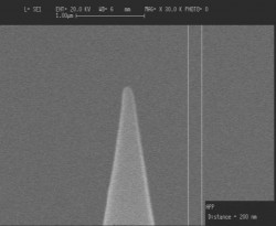
Noncontact Diamond Coated Conductive Probes DCP20 series, resonant frequency 260-630kHz, force constant 28-91N/m.
Coating Specification:
- Thickness of diamond coating is about 100 nm.
- Diamond coating is doped with nitrogen.
- Film resistivity: 0,5-1 Ohm*cm.
- Tip curvature radius after coating is about 100 nm.
- Recommended for electrical modes.
- Specially recommended for Oxidation Nanolithography*.
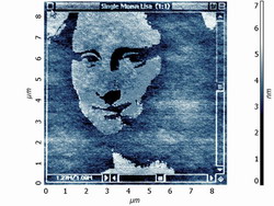
* We made a special "survival" test - almost 50 LAO Lithography images of Mona Lisa were obtained by using only one tip. It was not destroyed even after such a hard work. After 50 attempts it was still "alive".
|
LAO Nanolithography was made on Ti film in Semicontact mode by NSG20 probe with conductive diamond coating. NTEGRA Aura system. Scan size: 8x8µm. |
|
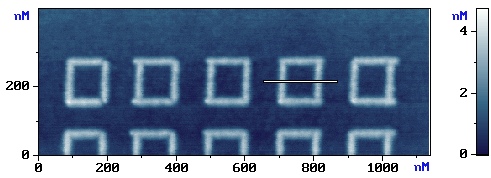
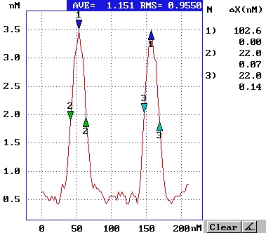
The thickness of lithography line was measured after the "survival" test.
It is about 22nm.
|
|
|
|
|
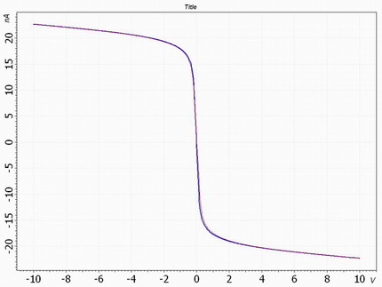
I/U characteristic made by DCP20 tip on freshly cleaved HOPG
|
Probe specification
- Standard chip size: 1.6x3.6x0.4 mm.
- High cemically stable reflective Au coating (reflective property is 3 times better in comparison with uncoated cantilevers).
- Typical curvature radius of a tip: 100 nm.
- Tip height: 10 - 15 µm.
- Each chip has one TRIANGULAR spring.
- Compatible with the most commercial SPM devices.
- Silicon is doped by boron with the concentration about 5x1020 cm-3 to avoid electrostatic charges.
- Packaged in GelPak® boxes.
GelPak® is a registered trade mark of Vichem Corporation.
| Specification for DCP20 series |
|
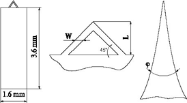 |
| Available Cantilever series | Cantilever length, L±5µm | Cantilever width, W±3µm | Cantilever thickness, µm | Resonant frequency, kHz | Force constant, N/m | ||||||
| min | typical | max | min | typical | max | min | typical | max | |||
| DCP20 | 90 | 60 | 1.7 | 2.0 | 2.3 | 260 | 420 | 630 | 28 | 48 | 91 |